Soitec and Resonac hook up to improve SiC yield and productivity
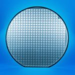
by David Manners · Electronics Weekly.comResonac (formerly Showa Denko K.K.) and Soitec are to co-develop 200mm (8-inch) SmartSiC wafers using Resonac substrates and epitaxy processes, in a move towards deployment of Soitec’s SiC technology in Japan and other international markets.
“Silicon carbide yield and productivity must be improved,” says Soitec CTO Christophe Maleville, “associating Resonac premium quality SiC materials with Soitec’s 200mm SmartSiC technology will support volume availability of record quality epi-ready substrate.”
“By combining Resonac’s high-quality monocrystalline silicon carbide wafers with Soitec’s SmartSiC
technology, we will deliver improved production efficiency of 200mm silicon carbide wafers and diversify the epi-wafer supply chain, ” says Resonac’s Makoto Takeda.
Soitec’s SmartSiC wafers are produced using the company’s proprietary SmartCut technology to bond an layer of mono SiC ‘donor’ wafer to a low-resistivity polycrystalline (poly-SiC) ‘handle’ wafer.
By allowing multiple re-uses of the prime quality mono-SiC wafer, the process reduces overall energy consumption during wafer manufacturing.
Soitec has a new plant at its headquarters in Bernin, France, primarily dedicated to the production of SmartSiC wafers.